EUV Lithography Explained: Unlocking the Next Generation of AI Chips
The cutting edge of AI hardware, from powerful GPUs to custom NPUs, relies on ever-shrinking transistors. But this miniaturization is gated by an incredibly complex process: Extreme Ultraviolet (EUV) Lithography. Understanding this technology is key to grasping why advanced AI chips are so expensive and difficult to acquire.
Krapton EngineeringReviewed by a senior engineer9 min readSemiconductors
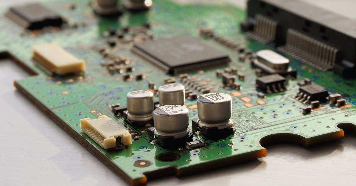
If you're building or scaling AI infrastructure in 2026, you've likely encountered the stark reality: state-of-the-art AI accelerators are expensive, and lead times can be unpredictable. This isn't just about demand outstripping supply; it's rooted deep in the intricate, multi-billion-dollar world of semiconductor manufacturing. At the heart of this bottleneck lies Extreme Ultraviolet (EUV) Lithography, a technology so complex and critical that a single company holds the key to the future of advanced chip production.
TL;DR: EUV lithography is the cutting-edge technology using ultra-short wavelength light to print the minuscule features required for 3nm and smaller process nodes, essential for high-performance AI chips. Its immense cost, technical complexity, and the near-monopoly of ASML in producing these machines are primary drivers of high AI hardware prices and supply constraints.
Key takeaways

- EUV lithography is indispensable for manufacturing chips at 3nm and beyond, powering the most advanced AI accelerators.
- ASML, a Dutch company, is the sole producer of commercial EUV machines, making it a critical choke point in the global semiconductor supply chain.
- The extreme cost and complexity of EUV tools contribute directly to the high price tags and limited availability of AI GPUs and custom silicon.
- As process nodes shrink, power density and thermal management become paramount, posing significant challenges for datacenter infrastructure.
- Next-generation High-NA EUV technology promises even finer resolution but will introduce further costs and manufacturing complexities.
What is EUV Lithography?

Extreme Ultraviolet (EUV) Lithography is the most advanced semiconductor manufacturing technique, enabling the creation of integrated circuits with features just a few nanometers wide. Traditional optical lithography uses deep ultraviolet (DUV) light with a wavelength of 193 nanometers. To print smaller features, you need a shorter wavelength. EUV utilizes light at an astonishing 13.5 nanometers – approximately 14 times shorter than DUV – allowing for significantly finer detail and denser transistor packing.
The process is incredibly intricate. Instead of lenses, EUV machines use a series of highly polished mirrors to reflect the EUV light, as ordinary glass would absorb it. The light source itself is generated by firing a high-power laser at microscopic droplets of molten tin, creating plasma that emits EUV radiation. This requires a vacuum environment throughout the entire exposure process to prevent the EUV light from being absorbed by air. It's an engineering marvel, pushing the boundaries of physics and materials science.
The ASML Monopoly: Why One Company Holds the Key
The global semiconductor industry, particularly for leading-edge nodes, is critically dependent on one company: ASML Holding N.V. Based in the Netherlands, ASML is currently the only company capable of manufacturing commercial EUV lithography systems. Each machine is a behemoth, weighing over 180 tons, comprising more than 100,000 components, and costing upwards of $200 million USD. Their production is slow, with ASML delivering only dozens of these systems per year.
This near-monopoly position means that every foundry aiming for 3nm, 2nm, or future process nodes—TSMC, Samsung Foundry, and Intel Foundry Services—must acquire ASML's EUV machines. This creates a significant supply chain bottleneck. Analyst estimates suggest that ASML's limited output directly constrains the capacity of these foundries to produce advanced chips, impacting everything from smartphone processors to the highly sought-after AI GPUs. The complexity of these machines also means ongoing maintenance and specialized expertise are crucial, adding another layer of operational cost and dependence.
How EUV Enables 3nm (and Beyond): The Physics of Light
The fundamental principle of lithography resolution is governed by the Rayleigh criterion: Resolution = k1 * (λ / NA), where λ (lambda) is the wavelength of light, and NA is the numerical aperture of the optical system. To achieve finer resolutions, you either need a smaller wavelength (λ) or a larger numerical aperture (NA). EUV's 13.5nm wavelength is a massive leap from DUV's 193nm, enabling features that were previously impossible.
For the latest 3nm process nodes, EUV is essential. While older nodes used complex and expensive multi-patterning techniques (re-exposing the wafer multiple times) with DUV to achieve finer features, EUV simplifies this by printing layers in fewer steps, reducing manufacturing complexity and improving yield. Looking ahead, the industry is already developing High-NA EUV, which increases the numerical aperture to further shrink features, targeting 2nm and 1.8nm nodes. This next generation of EUV will be even more expensive and complex, pushing the limits of what's possible in chip design.
When NOT to use this approach
While EUV is vital for leading-edge performance, it's not universally applicable. For many applications, particularly those not requiring extreme computational density like IoT devices, automotive chips, or certain consumer electronics, older and more cost-effective DUV-based process nodes (e.g., 28nm, 16nm, 7nm) remain perfectly viable and offer better cost-per-transistor. Over-specifying an EUV-produced chip for a workload that doesn't demand it can lead to unnecessary expense and extended lead times without a commensurate performance benefit.
Like this article? Help us grow.
Choose Krapton as a preferred source on Google to see more of our engineering insights in Search. You only need to click once.
Why this matters for your budget
The impact of EUV lithography's cost and scarcity directly translates into the budgets of startups and enterprises deploying AI. Here's how:
- High GPU Prices: The most powerful AI GPUs (like NVIDIA's H100 or AMD's Instinct MI300X) are built on the most advanced process nodes, typically 4nm or 3nm, which require EUV. The cost of EUV machines, the low volume of chips produced per machine, and the intense demand all factor into their multi-thousand-dollar price tags.
- Extended Lead Times: Foundry capacity for EUV-produced wafers is limited. This means longer waiting periods for new hardware, impacting project timelines and forcing companies to optimize existing resources or pay premiums for immediate access. In a recent client engagement, we faced significant lead times on GPU clusters for a large-scale LLM training project, forcing us to re-architect our data ingestion pipelines to reduce the overall compute hours required, rather than waiting months for hardware.
- Custom Silicon Costs: Hyperscalers and large enterprises increasingly design custom AI silicon (e.g., Google's TPUs, AWS's Trainium/Inferentia). These, too, rely on EUV for their leading-edge performance. The NRE (Non-Recurring Engineering) costs for such chips are astronomical, partially due to the foundry access and EUV mask costs.
- Operational Expenditure: Even if you lease cloud AI instances, the underlying hardware's cost structure, including EUV's contribution, dictates the pricing models of providers like AWS, Google Cloud, and Azure. This means higher hourly rates for GPU instances. Our team measured the performance impact of leveraging a newer generation GPU for inference on a Next.js 15.2 App Router application with server components that called an external LLM API. The efficiency gains were clear, but the cost per inference had to be carefully balanced against throughput requirements.
Understanding these manufacturing realities allows you to make more informed decisions about your AI AI development services strategy, whether that's optimizing your cloud spend, considering alternative hardware, or planning for longer procurement cycles.
Practical Implications: Yields, Throughput, and the AI Bottleneck
The journey from a blank silicon wafer to a functional AI chip is fraught with challenges. Even with EUV, maintaining high yields (the percentage of functional chips per wafer) at sub-5nm nodes is incredibly difficult. Defects at the atomic scale can render an entire chip useless. Foundries like TSMC invest heavily in process optimization, but the inherent complexity of EUV adds to the risk.
Throughput—the number of wafers processed per hour—is another critical factor. While EUV machines are highly advanced, their throughput is still a limiting factor compared to DUV systems. This directly impacts how many advanced chips can be produced annually. The demand for AI accelerators, particularly with the rapid evolution of large language models, has created an unprecedented strain on this limited supply, pushing lead times for cutting-edge hardware to over a year in some cases, according to industry reports as of 2026.
For software engineers, this means that optimizing code for existing hardware, rather than simply waiting for the next generation, becomes paramount. Techniques like quantization, model pruning, and efficient data loading can extract more performance from available GPUs. In a project leveraging Postgres 16 with pgvector 0.7 for semantic search, we found that careful index tuning and query optimization could significantly reduce the load on our GPU-accelerated embedding generation service, effectively extending the lifespan of our existing hardware fleet.
The Road Ahead: High-NA EUV and Future Challenges
The semiconductor industry isn't standing still. The next frontier in lithography is High-NA EUV, which aims to further improve resolution by increasing the numerical aperture of the optical system. ASML has already shipped its first High-NA EUV prototype system, the Twinscan EXE:5000, to Intel Foundry Services. These machines promise to enable 2nm and 1.8nm process nodes, pushing transistor density even higher. However, they come with an even higher price tag, estimated to be over $350 million USD per machine, and introduce new engineering challenges.
Beyond manufacturing, the physical limits of power and thermal management are becoming critical. As transistors get smaller and more numerous, the power density of these chips increases exponentially. Datacenters must grapple with unprecedented cooling requirements and power delivery challenges. Deploying a new generation of AI accelerators might not just be about acquiring the chips, but about upgrading the entire datacenter infrastructure. This interplay between manufacturing capability and deployment reality will continue to shape the cost and availability of AI compute for the foreseeable future. Leveraging cloud engineering services can help businesses navigate these complex infrastructure demands.
| Technology | Wavelength (nm) | Resolution (nm) | Key Benefit | Current Status |
|---|---|---|---|---|
| DUV (193nm) | 193 | ~38-45 (with multi-patterning) | Cost-effective for mature nodes | Used for 7nm and older nodes |
| EUV | 13.5 | ~13-15 | Enables 3nm, 2nm; simplifies patterning | Essential for leading-edge AI chips (4nm, 3nm) |
| High-NA EUV | 13.5 | ~8 | Enables 2nm, 1.8nm with higher density | In development; first prototypes shipped |
FAQ
What is the biggest challenge in EUV lithography?
The biggest challenge is generating and controlling the 13.5nm EUV light. It requires extreme precision, a vacuum environment, and highly reflective mirrors, making the machines incredibly complex, expensive, and difficult to manufacture at scale.
Why is ASML the only company making EUV machines?
ASML invested decades and billions of dollars into R&D, overcoming immense technical hurdles in optics, vacuum technology, and light source generation. This created a significant technological barrier to entry that competitors have been unable to match.
How does EUV impact the cost of consumer electronics?
While EUV primarily affects high-end processors like AI GPUs and premium smartphone chips, its high manufacturing cost trickles down. These advanced components are more expensive, contributing to the higher price of devices that incorporate them.
What are process nodes (e.g., 3nm) and how do they relate to EUV?
Process nodes (like 3nm) refer to the manufacturing generation, indicating the typical feature size of transistors. EUV lithography is the key technology that enables foundries to achieve these incredibly small dimensions, allowing more transistors to be packed onto a chip for higher performance and efficiency.
Planning AI infrastructure around real hardware constraints? Talk to Krapton
Navigating the complexities of semiconductor supply chains and their direct impact on AI hardware availability and cost requires deep technical insight. Understanding the foundational technologies like EUV lithography is crucial for strategic planning. If your organization is designing, deploying, or optimizing AI solutions and needs to factor in the realities of the global chip market, our expert team can help. Book a free consultation with Krapton to discuss your specific needs.


