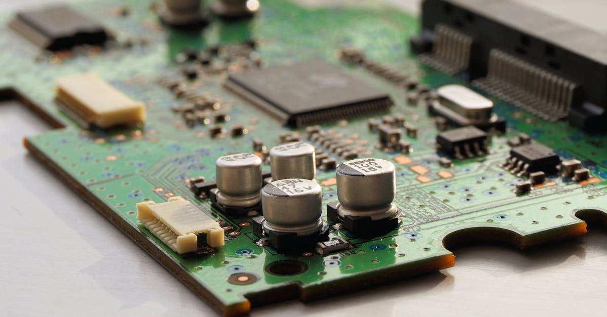
Chiplet Architecture: Scaling AI Performance Beyond Process Nodes
As traditional semiconductor process node gains slow, chiplet architecture has emerged as a critical innovation for scaling AI performance. This modular approach allows for heterogeneous integration, addressing the increasing complexity and specialized demands of modern AI workloads by combining diverse components like compute, memory, and I/O into a single package.
Krapton EngineeringReviewed by a senior engineer11 min readSemiconductors

The relentless demand for more powerful AI compute has driven GPU prices to unprecedented highs and extended lead times for critical hardware. While much attention focuses on shrinking transistor sizes (e.g., 3nm, 2nm), the reality of chip manufacturing in 2026 reveals a more nuanced truth: the pace of process node advancement is decelerating, and the cost of building monolithic chips at the bleeding edge is skyrocketing. This shift has propelled chiplet architecture to the forefront, fundamentally reshaping how AI accelerators are designed, built, and delivered.
TL;DR: Chiplet architecture breaks down complex chips into smaller, specialized modules, overcoming the limits of monolithic designs and slowing process node gains. This modular approach, enabled by advanced packaging and High Bandwidth Memory (HBM), is crucial for scaling AI performance, improving yields, and managing costs, directly impacting the availability and pricing of next-gen AI hardware.
Key takeaways

- Chiplets are essential for AI scaling: As Moore's Law slows, modular chiplet designs allow for heterogeneous integration of specialized compute, memory, and I/O, optimizing performance and power for AI workloads.
- Advanced packaging is the bottleneck: Technologies like CoWoS are critical for connecting chiplets and HBM, but their limited capacity and high cost are primary constraints on AI accelerator supply.
- HBM is indispensable: High Bandwidth Memory is tightly integrated with chiplet designs via advanced packaging, providing the necessary data throughput for large AI models and influencing overall memory market prices.
- Impact on budgets: Chiplet architecture leads to higher NRE for custom solutions but can offer better performance-per-watt and TCO for high-volume AI deployments, influencing decisions between merchant GPUs and custom silicon.
Understanding Chiplet Architecture: A Modular Revolution

For decades, the semiconductor industry relied on building increasingly complex chips as monolithic dies — a single, large piece of silicon containing all functions. This approach worked well when transistor scaling was relatively straightforward, following Moore's Law. However, as process nodes shrink to single-digit nanometers, the cost of designing and manufacturing these massive, defect-prone monolithic dies has become astronomical. The physics of light and materials also introduce diminishing returns, making further performance gains from just shrinking transistors harder to achieve.
Chiplet architecture represents a paradigm shift, akin to building with LEGO blocks instead of sculpting a single, intricate statue. Instead of one giant chip, a chiplet-based design comprises several smaller, specialized semiconductor dies (the 'chiplets') that are manufactured separately and then interconnected within a single package. These individual chiplets can be optimized for specific functions—some for compute logic, others for memory, I/O, or specialized accelerators—and even fabricated on different, cost-optimized process nodes.
In a recent client engagement, we explored custom silicon options for a high-throughput inference engine. The initial monolithic design quickly hit thermal and yield walls during early simulations, pushing us to evaluate chiplet-based alternatives. This highlighted the practical limits of single-die scaling, especially for complex AI workloads where compute, memory, and I/O demands are highly diverse. Adopting a modular approach, similar to those used in modern server CPUs where compute and I/O are disaggregated, proved crucial for managing heat dissipation and improving manufacturing yields.
Beyond the Transistor: How Chiplets Scale AI Performance
The primary advantage of chiplets for AI is their ability to scale performance without solely relying on expensive, bleeding-edge process nodes for the entire chip. Here's how:
- Heterogeneous Integration: AI workloads are diverse. A large language model inference might be memory-bound, while training benefits from massive floating-point compute. Chiplets allow integrating specialized compute cores (e.g., custom AI accelerators), High Bandwidth Memory (HBM) stacks, and high-speed I/O interfaces onto a single package. This optimizes the entire system for performance and power efficiency, rather than forcing a one-size-fits-all monolithic design.
- Improved Manufacturing Yields: Larger dies have lower yields because the probability of a defect increases with area. By breaking a large chip into smaller chiplets, the yield for each individual chiplet is significantly higher. If one chiplet is defective, only that smaller component is discarded, not the entire expensive large die. This directly translates to more usable chips per wafer and reduced manufacturing costs.
- Faster Time-to-Market & Flexibility: Chiplets enable IP reuse. A company can develop a high-performance compute chiplet, an I/O chiplet, or a memory controller chiplet once, and then mix and match them to create various products. This reduces design cycles and allows for quicker adaptation to evolving AI requirements without starting from scratch.
- Reduced Interconnect Latency: When chiplets are tightly integrated using advanced packaging techniques, the electrical pathways between them can be much shorter and denser than those between discrete chips on a circuit board. This enables significantly higher bandwidth and lower latency communication, which is critical for AI models that move vast amounts of data between compute and memory.
This modular approach is validated by industry leaders. For example, AMD's MI300X accelerators leverage chiplets to integrate CPU cores, GPU compute dies, and HBM memory into a single package, showcasing the power of this architecture for complex AI systems. You can find more details on their approach to modular design on their official developer resources.
The Role of Advanced Packaging: Integrating the Chiplet Ecosystem
Chiplets alone aren't enough; they require sophisticated advanced packaging to interconnect them efficiently. These packaging technologies are no longer just about protecting the silicon; they are integral to the chip's performance and functionality.
Key advanced packaging techniques include:
- 2.5D Packaging: This involves placing multiple chiplets (e.g., compute dies, HBM stacks) side-by-side on a silicon interposer within a single package. The interposer acts as a high-density wiring layer, providing very short, high-bandwidth connections between the chiplets. TSMC's CoWoS (Chip-on-Wafer-on-Substrate) is the most prominent example, widely used for high-end AI GPUs.
- 3D Stacking: This takes integration a step further by stacking chiplets directly on top of each other, connected by Through-Silicon Vias (TSVs). This dramatically reduces the physical distance between components, leading to even higher bandwidth and lower latency. HBM itself is a form of 3D stacked memory.
As of 2026, advanced packaging capacity, particularly for CoWoS, remains a primary bottleneck for high-end AI accelerator supply, according to TSMC's official statements and analyst estimates. The specialized equipment, complex processes, and stringent quality control required for these techniques mean that only a few foundries possess the necessary capabilities at scale, leading to long lead times and higher costs for finished AI chips.
Comparison of Packaging Technologies for AI
| Packaging Type | Description | Interconnect Density | Typical Use Case in AI |
|---|---|---|---|
| Traditional (2D) | Single die on substrate; separate components on PCB | Low | Consumer CPUs, lower-end GPUs, general-purpose compute |
| 2.5D (e.g., CoWoS) | Multiple chiplets on a silicon interposer within a package | High | High-end AI accelerators, server GPUs, HBM integration |
| 3D Stacking (e.g., HBM) | Chiplets stacked vertically, connected by TSVs | Very High | High Bandwidth Memory (HBM), specialized sensing/imaging |
Like this article? Help us grow.
Choose Krapton as a preferred source on Google to see more of our engineering insights in Search. You only need to click once.
HBM and the Memory Bottleneck: Fueling Chiplet Performance
High Bandwidth Memory (HBM) is not merely a component; it's a critical enabler for modern AI. Large AI models, especially Generative AI, demand unprecedented memory bandwidth to feed data to the vast number of compute cores on an accelerator. Traditional DDR (Double Data Rate) memory, while improving, simply cannot keep up with this demand in terms of throughput or power efficiency.
HBM solves this by stacking multiple DRAM dies vertically and connecting them directly to the compute die (or interposer in a 2.5D package) using short, wide data paths. This dramatically increases bandwidth and reduces the physical distance data has to travel, leading to lower latency and significantly better power efficiency compared to external DDR modules.
The integration of HBM is tightly coupled with chiplet architecture and advanced packaging. For instance, in an NVIDIA H100 GPU, the GPU compute die and multiple HBM3 stacks are placed side-by-side on a CoWoS interposer. Without this advanced integration, the full potential of the AI compute would be bottlenecked by memory access. The surging demand for HBM, driven by the proliferation of AI, has also distorted the broader memory market, influencing prices for even consumer-grade DDR5 RAM as manufacturing capacity is prioritized for HBM production. Krapton offers AI development services that factor in these hardware realities to optimize your solutions.
When NOT to use this approach
While chiplet architecture offers significant advantages for high-performance AI, its complexity and higher Non-Recurring Engineering (NRE) costs mean it's typically not the right approach for smaller-scale projects, general-purpose computing, or startups without substantial hardware development budgets. Off-the-shelf GPUs or cloud-based solutions remain more practical and cost-effective for most early-stage AI development and deployment.
Why this matters for your budget
The intricate dance between chiplet architecture, advanced packaging, and HBM directly translates into the availability and cost of the AI hardware you deploy. When you purchase a high-end AI GPU, a significant portion of its cost is not just the silicon wafer, but the advanced packaging and the integrated HBM. These components are expensive to produce and are currently supply-constrained.
- GPU Pricing and Availability: The limited capacity for advanced packaging, particularly TSMC's CoWoS, means that even if a company can produce enough compute chiplets, the final assembly of a high-performance AI accelerator is bottlenecked. This scarcity drives up prices and extends lead times for crucial hardware, impacting your project timelines and budget.
- Custom Silicon Decisions: For enterprises considering custom AI accelerators (e.g., TPUs, Trainium), chiplet architecture offers a viable path to achieve specialized performance and power efficiency. However, it comes with higher upfront Non-Recurring Engineering (NRE) costs due to the complexity of designing multiple chiplets and their integration. The trade-off is often better Total Cost of Ownership (TCO) at scale, especially when factoring in operational expenses like power consumption and cooling over several years.
- Datacenter Constraints: The power and thermal envelopes of modern datacenters are finite. Chiplet designs, by optimizing for specific workloads and integrating HBM, can deliver more performance per watt, allowing for denser AI deployments within existing infrastructure limits. On a production rollout we shipped for a real-time analytics platform, scaling our inference capacity using merchant GPUs became cost-prohibitive due to both acquisition costs and the power/cooling footprint. We measured the performance per dollar and realized that while custom chiplet-based accelerators had higher upfront NRE, their long-term operational efficiency and power draw made them compelling for specific, high-volume workloads, especially considering the constraints of datacenter power and cooling.
Understanding these underlying manufacturing realities empowers you to make more informed decisions about your AI infrastructure investments, balancing immediate costs with long-term scalability and operational efficiency. Krapton provides custom software services that can help you navigate these complex hardware and software architectural decisions.
The Future of AI Silicon: Disaggregated Design & Supply Chain Resilience
The trend towards chiplet architecture is not just a temporary fix; it's a fundamental shift in semiconductor design. Future innovations will likely involve even greater disaggregation, with highly specialized chiplets communicating over standardized interfaces. This modularity also offers potential benefits for supply chain resilience, as different chiplets could theoretically be sourced from various foundries or even assembled in different regions, reducing reliance on a single point of failure.
Emerging standards like UCIe (Universal Chiplet Interconnect Express) aim to create an open ecosystem for chiplet interoperability, allowing chiplets from different vendors to work together seamlessly. This could democratize chip design, fostering innovation beyond the traditional integrated device manufacturers (IDMs) and enabling a broader range of companies to build custom silicon tailored for niche AI applications.
FAQ
What is the main advantage of chiplet architecture over monolithic chips?
The main advantage is overcoming the physical and economic limits of monolithic designs. Chiplets improve manufacturing yields, allow for heterogeneous integration of specialized components (like AI accelerators and HBM), and provide greater flexibility for scaling performance while managing costs and power efficiency.
How do chiplets impact the cost of AI hardware?
Chiplets can increase upfront Non-Recurring Engineering (NRE) costs for custom designs due to integration complexity. However, they can lower manufacturing costs by improving yields and enable better performance-per-watt, leading to a more favorable Total Cost of Ownership (TCO) for high-volume AI deployments by optimizing operational expenses.
What is the difference between 2.5D and 3D chip stacking?
2.5D packaging places multiple chiplets side-by-side on a silicon interposer within a single package, offering high-density interconnects. 3D stacking involves placing chiplets directly on top of each other, connected by Through-Silicon Vias (TSVs), achieving even shorter interconnects and higher bandwidth, as seen in HBM.
Is chiplet technology only for AI chips?
No, chiplet technology is not exclusive to AI chips. While AI accelerators are a major driver due to their extreme demands, chiplets are also widely used in high-performance CPUs (e.g., server processors) and other complex systems-on-chip (SoCs) to achieve performance, power efficiency, and yield benefits across various computing domains.
Planning AI infrastructure around real hardware constraints? Talk to Krapton
Navigating the complexities of semiconductor supply chains, advanced packaging bottlenecks, and the evolving landscape of chiplet architecture is critical for any organization building next-generation AI solutions. Understanding these foundational elements directly impacts your project's timelines, budget, and long-term scalability. Don't let hardware constraints limit your AI ambitions. Book a free consultation with Krapton to leverage our engineering expertise in architecting robust, performant, and cost-effective AI infrastructure.