Advanced Chip Packaging: Decoding AI Performance & Hardware Costs
The demand for AI accelerators is skyrocketing, but the real bottleneck isn't just process nodes. Advanced chip packaging, like TSMC's CoWoS, and High Bandwidth Memory (HBM) are now the critical factors determining performance, availability, and cost in the semiconductor supply chain. Dive deep into the engineering realities shaping AI hardware.
Sahil ChaudharyReviewed by a senior engineer12 min readSemiconductors
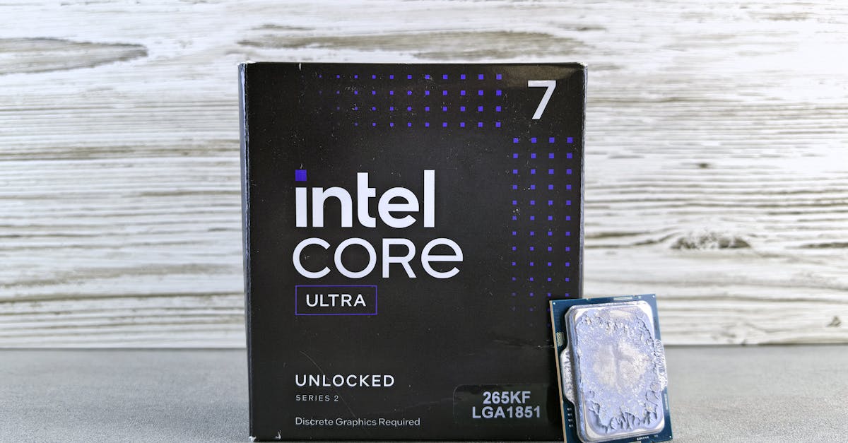
As builders and engineers, we’ve all felt the pinch: the latest AI GPUs are incredibly powerful, yet consistently expensive, hard to acquire, or carry surprisingly long lead times. While the 'nanometer wars' of process nodes capture headlines, the true chokepoint for AI accelerators in 2026 often lies elsewhere. The secret to unlocking next-generation AI performance – and understanding the underlying hardware costs – is increasingly found in sophisticated manufacturing techniques like advanced chip packaging and High Bandwidth Memory (HBM).
TL;DR: Advanced chip packaging, particularly 2.5D solutions like TSMC’s CoWoS, and High Bandwidth Memory (HBM) are now the primary drivers of AI accelerator performance, cost, and availability. As traditional process node scaling slows, these innovations are critical for integrating logic and memory to meet AI's insatiable demand for bandwidth, directly impacting everything from GPU prices to cloud compute costs.
Key takeaways

- Process Node Slowdown: Shrinking transistor sizes (e.g., 3nm) offers diminishing returns, shifting performance gains to advanced chip packaging.
- Advanced Packaging is Key: Techniques like TSMC's CoWoS (Chip-on-Wafer-on-Substrate) enable 2.5D integration, dramatically improving communication between logic and memory.
- HBM is Critical: High Bandwidth Memory (HBM) provides vastly superior bandwidth and power efficiency compared to traditional DDR5, essential for AI workloads.
- Supply Chain Bottleneck: Advanced packaging capacity, especially for CoWoS, is currently more constrained than basic wafer fabrication, limiting AI accelerator output.
- Budget Impact: These manufacturing realities directly translate to higher GPU prices, longer lead times, and increased cloud AI inference costs.
The New Bottleneck: Why Advanced Chip Packaging Reigns Supreme for AI

For decades, Moore's Law dictated that the number of transistors on a microchip would double approximately every two years. This relentless scaling, primarily driven by shrinking process nodes (like moving from 7nm to 3nm), delivered consistent performance and efficiency gains. However, the physics are getting harder. Transistor density gains are slowing, and the cost per transistor is no longer reliably decreasing at the same rate. This shift means that while smaller nodes still offer benefits, they are no longer the sole or even primary lever for innovation.
Enter advanced chip packaging. Instead of just making transistors smaller, advanced packaging focuses on how different chip components – like the main processing logic (GPU or CPU) and high-speed memory – are physically connected and integrated. For AI workloads, which demand massive data throughput and parallel processing, the ability to rapidly move data between the compute units and memory is paramount. Traditional packaging methods simply can't keep up with this demand, leading to a phenomenon known as the "memory wall."
Advanced packaging technologies overcome this wall by bringing components much closer together, enabling wider, faster, and more energy-efficient communication paths. This is why you see cutting-edge AI accelerators leveraging solutions that go far beyond standard surface-mount techniques. It's not just about what's on the chip, but how the chips are put together.
CoWoS Explained: TSMC's Answer to AI's Insatiable Demands
One of the most prominent and critical advanced packaging technologies for AI is TSMC's CoWoS (Chip-on-Wafer-on-Substrate). This technique is a form of 2.5D packaging, a bridge between traditional 2D planar chips and true 3D stacking. CoWoS addresses the challenge of integrating multiple heterogeneous dies (e.g., a large AI processor and several HBM stacks) into a single package with high bandwidth and low latency.
Here’s a simplified breakdown of how CoWoS works:
- Interposer: Instead of directly mounting chips onto a standard PCB, CoWoS uses a silicon interposer. This interposer is essentially a small, highly advanced silicon wafer, often built using mature process nodes, that acts as a super-dense wiring board.
- Through-Silicon Vias (TSVs): The interposer contains thousands of tiny vertical electrical connections called Through-Silicon Vias (TSVs). These TSVs pass directly through the silicon, connecting the top surface (where the logic and memory dies are placed) to the bottom surface (which connects to the package substrate).
- Micro-Bumps: The logic die (e.g., an NVIDIA H100 GPU die or an AMD MI300X) and the HBM memory stacks are connected to the interposer using extremely fine-pitch micro-bumps. These bumps provide a very dense array of electrical contacts, enabling a vast number of parallel data paths.
- Substrate Integration: The interposer, with its mounted dies, is then attached to a larger organic package substrate, which provides the final connections to the circuit board.
The CoWoS approach allows the GPU and HBM stacks to be placed side-by-side on the interposer, creating extremely short, wide, and fast communication channels. This drastically reduces signal latency and power consumption compared to routing signals across a traditional PCB. TSMC's mastery of CoWoS, particularly its CoWoS-S variant, has made it a crucial gatekeeper for high-performance AI accelerators, as very few foundries possess the equivalent capabilities and capacity. According to industry analysts, TSMC's CoWoS capacity has been a primary bottleneck for AI GPU supply through 2024 and 2025, with expansion efforts ongoing into 2026.
Beyond CoWoS: The Future of 3D Stacking
While 2.5D packaging like CoWoS is prevalent today, true 3D stacking involves vertically integrating different chip layers directly on top of each other, sharing an even denser array of TSVs. Examples include stacking multiple layers of cache memory directly onto a CPU die or stacking logic and memory. This offers even greater density and shorter interconnects but introduces significant challenges, particularly thermal management (heat from lower layers can affect upper layers) and yield (a defect in any layer can spoil the whole stack). However, advancements in hybrid bonding and micro-bump technology are pushing 3D stacking closer to mainstream adoption for certain applications.
Like this article? Help us grow.
Choose Krapton as a preferred source on Google to see more of our engineering insights in Search. You only need to click once.
High Bandwidth Memory (HBM): The Unsung Hero of AI Accelerators
You can have the fastest GPU in the world, but if it can't get data fast enough, its compute units will sit idle. This is where High Bandwidth Memory (HBM) comes in. HBM is a revolutionary type of RAM specifically designed to provide extremely high data throughput with low power consumption, making it indispensable for AI, high-performance computing (HPC), and graphics.
Unlike traditional DRAM modules (like DDR5) that communicate via a relatively narrow bus (e.g., 64-bit per module), HBM stacks multiple DRAM dies vertically, connecting them with thousands of TSVs to a wide interface (typically 1024-bit per stack). This parallel architecture dramatically increases bandwidth.
The latest iterations, such as HBM3E and the upcoming HBM4 standard from JEDEC, push bandwidth into the terabytes-per-second range for a single accelerator. This colossal bandwidth is critical for feeding the massive matrix multiplications and tensor operations that define modern AI models, especially large language models (LLMs) and complex neural networks.
To illustrate the difference, consider this comparison:
| Feature | DDR5 (Consumer/Server RAM) | HBM3 (AI/HPC Memory) |
|---|---|---|
| Interface Width (per module/stack) | 64-bit | 1024-bit |
| Peak Bandwidth (per module/stack) | ~50-60 GB/s | ~800-900 GB/s (per stack) |
| Power Efficiency | Good | Excellent (lower energy per bit) |
| Physical Footprint | Larger (DIMMs) | Very Small (stacked dies, on-package) |
| Primary Use Case | General computing, consumer PCs, servers | AI accelerators, HPC, high-end GPUs |
HBM & The Memory Market: Why Your Consumer RAM is Affected
The immense demand for HBM from AI accelerator manufacturers has a ripple effect across the entire DRAM market. HBM production consumes a significant portion of advanced DRAM wafer capacity. Memory manufacturers, incentivized by higher profit margins on HBM, prioritize its production. This redirection of resources can tighten the supply of standard DDR5 DRAM used in consumer PCs and general-purpose servers, leading to price increases or slower adoption of newer, faster modules.
In a recent client engagement building a real-time inference pipeline with a custom LLM, we encountered significant VRAM bottlenecks when attempting to load models larger than 80GB on a single GPU. The primary constraint wasn't the compute units, but the available HBM capacity and bandwidth on the chosen accelerator, directly impacting our ability to serve concurrent requests efficiently. This forced us to optimize model quantization and batching strategies, which added complexity to the deployment.
The Foundry Landscape: Capacity, Yields, and Geopolitical Realities
The global semiconductor manufacturing landscape is dominated by a few key players: TSMC, Samsung Foundry, and increasingly, Intel Foundry. While these companies are investing heavily in new wafer fabrication plants (fabs) for leading-edge process nodes (like 3nm and 2nm), the critical bottleneck for AI accelerators has often been the capacity for advanced packaging, especially CoWoS.
Building a new fab takes years and tens of billions of dollars. Expanding advanced packaging lines, while also capital-intensive, is a distinct challenge. The specialized equipment and expertise required for processes like TSV formation, micro-bumping, and die-to-interposer bonding are highly concentrated. TSMC, for instance, has been working aggressively to expand its CoWoS capacity, but demand continues to outstrip supply, leading to long lead times for AI hardware from companies like NVIDIA and AMD.
Geopolitical factors and export controls further complicate the supply chain. Governments are increasingly viewing semiconductor manufacturing, particularly advanced nodes and packaging, as a matter of national security. This can influence where fabs are built, what equipment can be purchased, and which markets can be served, adding layers of complexity and potential delays to hardware availability. Our team, evaluating a GPU cluster for a large-scale computer vision project using PyTorch 2.3 and CUDA 12.3, measured a significant drop in effective throughput when data transfer rates exceeded the HBM bandwidth, even with ample compute. Optimizing data pipelines to minimize repeated memory access and leveraging techniques like mixed-precision training became crucial to fully utilize the expensive silicon, highlighting the memory subsystem's critical role.
Why this matters for your budget
For founders, product managers, and engineers planning AI infrastructure, understanding advanced chip packaging is no longer an academic exercise; it's a critical input to strategic decisions:
- GPU Costs & Availability: The high cost and scarcity of AI GPUs are directly tied to the complexity and limited capacity of advanced packaging and HBM production. If you're buying hardware or provisioning cloud instances (e.g., AWS EC2 P5 instances with H100s or Google Cloud TPUs), you're paying a premium for this cutting-edge integration.
- Cloud vs. On-Premise: The decision to deploy AI workloads in the cloud versus on-premise is heavily influenced by the availability and cost of these specialized accelerators. Cloud providers leverage their scale to secure supply, but you still pay a premium.
- Performance Expectations: Knowing that HBM bandwidth is often the true performance limiter, not just FLOPS, informs how you design and optimize your AI models. Efficient data loading, quantization, and memory management become paramount.
- Strategic Planning: For enterprises considering custom AI silicon (TPUs, Trainium, Maia), understanding advanced packaging is essential. It's not enough to design a great chip; you need a reliable path to manufacture and package it, which often means navigating the same constrained supply chains. For expert guidance on navigating these complexities, explore our AI development services.
When NOT to rely solely on process node shrinks
While smaller process nodes deliver density and power efficiency, blindly chasing the latest 'nm' number isn't always the optimal strategy. For many general-purpose computing tasks, or even some AI inference workloads that are not heavily memory-bound, a mature 7nm or 5nm process combined with robust architectural optimizations can be more cost-effective and readily available than the bleeding-edge 3nm or 2nm nodes with their associated packaging complexities. The yield challenges and astronomical costs of the newest nodes mean that the overall cost-performance-power (PPA) benefit might not justify the investment for every use case. Strategic decisions should weigh workload requirements against the real-world manufacturing and supply chain realities of leading-edge silicon.
FAQ: Your Questions on Advanced Chip Packaging Answered
What is the difference between 2.5D and 3D packaging?
2.5D packaging, like CoWoS, places multiple dies (logic, memory) side-by-side on a silicon interposer, which then connects to a substrate. 3D packaging involves directly stacking multiple active dies on top of each other, often connected by TSVs, offering even greater density but posing more significant thermal and manufacturing challenges.
Why is CoWoS so important for AI?
CoWoS is crucial for AI because it enables extremely high-bandwidth, low-latency communication between powerful AI processors and HBM. This integration drastically reduces the "memory wall" bottleneck, allowing AI accelerators to process vast amounts of data quickly and efficiently, which is vital for modern neural networks and LLMs.
How does HBM compare to GDDR memory?
HBM (High Bandwidth Memory) typically offers a much wider interface (1024-bit vs. 384-bit for GDDR6) and higher bandwidth per pin, making it more power-efficient for a given bandwidth. GDDR (Graphics Double Data Rate) is generally cheaper, has higher raw clock speeds, and is more common in consumer GPUs, offering a good balance for gaming and less memory-intensive AI tasks.
What role do chiplets play in advanced packaging?
Chiplets are individual functional blocks (e.g., CPU cores, I/O controllers, GPU tiles) manufactured separately and then integrated into a single package using advanced packaging. This modular approach allows for mixing and matching different process nodes, improving yield, and creating highly customized, powerful processors more efficiently than a single monolithic die.
Are advanced packaging bottlenecks easing?
While major foundries like TSMC are aggressively expanding advanced packaging capacity into 2026, demand for AI accelerators continues to grow rapidly. The bottleneck is slowly easing but remains a significant factor in lead times and costs for the most advanced AI hardware. Predicting a complete easing is challenging given the dynamic nature of AI demand.
Planning AI Infrastructure Around Real Hardware Constraints? Talk to Krapton
Navigating the complex world of AI hardware and semiconductor supply chains requires deep technical insight and strategic foresight. Whether you're building a new SaaS product with AI capabilities, optimizing existing ML inference, or scaling your enterprise AI infrastructure, understanding these underlying manufacturing realities is key. Don't let hardware bottlenecks slow your innovation. Book a free consultation with Krapton to discuss your custom software and AI integration needs, and let our expert engineers help you build for performance and scalability.


